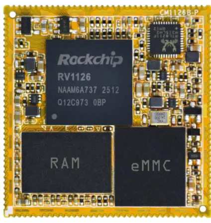
Papatono Whakamaua CM1126B-P Pūnaha ki te Kōwae
Whakatakotoranga
| Āhuahira | Whakatakotoranga |
| PTM | Cortex-A53-matua |
| DDR | 2GB LPDDR4 (tae atu ki te 4GB) |
| eMMC FLASH | 8GB (tae atu ki te 256GB) |
| Mana | DC 3.3V |
| MIPI DSI | 4-Rae |
| I2S | 4-CH |
| MIPI CSI | 2-CH 4-Rae |
| RGB LCD | 24bit |
| Kāmera | 1-CH(DVP) me 2-CH(CSI) |
| USB | 2-CH (USB HOST 2.0 me OTG 2.0) |
| Itarangi | 1000M GMAC |
| SDMMC | 2-CH |
| I2C | 5-CH |
| SPI | 2-CH |
| UART | 5-CH, 1-CH(DEPUG) |
| PWM | 11-CH |
| ADC IN | 4-CH |
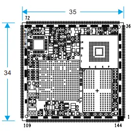
| Ahu Poari | 34 x 35mm |
Kupu Whakataki
Mo tenei pukapuka
Ko te tikanga o tenei pukapuka hei whakarato ki te kaiwhakamahi ki rungaview o te poari me ona painga, te whakaoti i nga waahanga, me nga tikanga whakarite. Kei roto hoki nga korero haumaru nui.
He urupare me te whakahou ki tenei pukapuka
Hei awhina i o taatau kaihoko ki te whai hua i a maatau hua, kei te mahi tonu matou i nga rauemi taapiri me te whakahou kia waatea i runga i te Poari webpae (www.boardcon.com, www.armdesigner.com). Kei roto i enei ko nga pukapuka pukapuka, nga korero tono, nga papatono examples, me te whakahou i nga rorohiko me nga taputapu. Takitaki i ia wa kia kite he aha nga mea hou! I a matou e aro nui ana ki nga mahi mo enei rauemi kua whakahoutia, ko nga urupare mai i nga kaihoko te awe tuatahi, Mena he patai, he korero, he awangawanga ranei mo to hua, kaupapa ranei, tena koa waea mai ki a matou i support@armdesigner.com.
CM1126B-P Whakataki
Whakarāpopototanga
Ko te CM1126B-P system-on-module he mea whakauru ki te Rockchip's RV1126B-P, i hangaia me te quad-core Cortex-A53, 3.0 TOPs NPU, me te RISC-V MCU. He mea hanga motuhake mo nga taputapu IPC/CVR, nga taputapu AI Camera, nga taputapu whakawhitiwhiti mohio, me nga robots paku. Ka taea e nga otinga mahi teitei me te iti-hiko te awhina i nga kaihoko ki te whakauru tere ake i nga hangarau hou me te whakarei ake i te pai o te otinga. Ko te rahi iti ka taea te whakanoho ki runga i te papa 38. Whai muri i te whakahoutanga o nga taputapu mai i te CM1126 (V1) ki te CM1126B-P (V2), kei reira te SoC e whakahouhia ana ki te RV1126B-P, nga tohu Tautuhi & OTG_VBUS me te WIFI/BT module's GPIO voltagme mahi i te taumata arorau 3.3V.
Ngā āhuatanga
Tukatuka moroiti
- Quad-core Cortex-A53 ki runga ki te 1.6GHz
- 32KB I-keteroki me te 32KB D-keteroki mo ia matua, 512KB L3 keteroki
- 3.0 TOPS Waeine Tukatuka Neural
- RISC-V MCU ki te tautoko i te 250ms te peke tere
- Morahi 12M ISP
Whakahaere Mahara
- LPDDR4 RAM ki te 4GB
- eMMC ki te 256GB
- SPI Flash ki runga ki te 8MB
Kaiwaehere Ataata/Whakawaehere
- Ka tautokohia te wetewaehere/whakawaehere ataata ki te 4K@30fps
- E tautoko ana i te wa-tūturu wetewaehere o H.264/265
- E tautoko ana i te wa-tūturu UHD H.264/265 whakawaehere ataata
- Te rahi o te pikitia ki te 8192×8192
Whakaatu Pūnaharoto
- Putanga Ataata
- Ka tautokohia nga huarahi 4 MIPI DSI ki te 2560x1440@60fps
- E tautoko ana i te putanga whakarara RGB 24-bit
- Whakaahua i roto
- Tautoko ake ki te 16-bit atanga DVP
- Ka tautokohia te atanga 2ch MIPI CSI 4lanes
I2S/PCM/AC97
- E toru atanga I2S/PCM
- Tautokohia te huinga Mic ki te 8ch atanga PDM/TDM
- Tautokohia te putanga ororongo PWM
USB me te PCIE
- E rua nga atanga USB 2.0
- Kotahi USB 2.0 OTG me tetahi 2.0 USB ope
Itarangi
- RTL8211F kei runga
- Tautoko 10/100/1000M
I2C
- Tae atu ki te rima I2C
- Tautokohia te aratau paerewa me te aratau tere (tae atu ki te 400kbit/s)
SDIO
- Tautokohia te kawa 2CH SDIO 3.0
SPI
- Tae atu ki te rua nga kaiwhakahaere SPI,
- Atanga rangatū tukutahi-katoa
UART
- Tautoko ki te 6 UART
- UART2 me nga waea e 2 mo nga taputapu patuiro
- E rua nga FIFO 664-paita kua whakauruhia
- Tautokohia te aratau rere aunoa mo UART0/1/3/4/5
ADC
- Kia wha nga hongere ADC
- 12-bit taumira
- Voltage awhe whakauru i waenga i te 0V ki te 1.8V
- Tautoko ake ki te 1MS/ssampreiti ling
PWM
- 11 nga PWM maramara me te mahi haukoti
- Tautoko moka-32-wa / whare porotiti
- Kōwhiringa IR i runga i te PWM3/7
Wae hiko
- Te Mana Motuhake i runga i te papa
- Takitahi 3.3V whakauru
CM1126B-P Hoahoa Poraka
RV1126B-P Hoahoa Poraka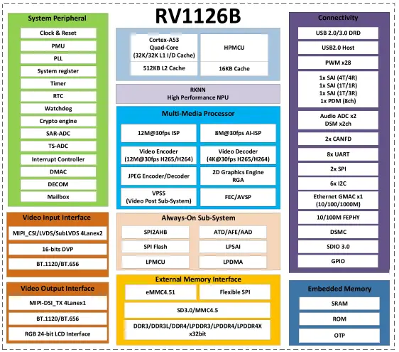
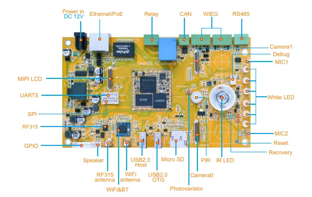
Papa Whanaketanga (Idea1126) Hoahoa Poraka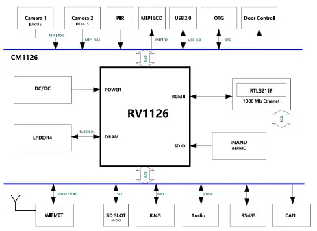
CM1126B-P PCB Ahu
CM1126B-P Whakamaramatanga Pin
| Pin | Waitohu | Whakaahuatanga, mahi ranei | rangatū GPIO | IO Voltage |
| 1 | LCDC_D19_3V3 | I2S1_MCLK_M2/CIF_D15_M1 | GPIO2_C7_d | 3.3V |
| 2 | LCDC_D20_3V3 | I2S1_SDO_M2/CIF_VS_M1 | GPIO2_D0_d | 3.3V |
| 3 | LCDC_D21_3V3 | I2S1_SCLK_M2/CIF_CLKO_M1 | GPIO2_D1_d | 3.3V |
| 4 | LCDC_D22_3V3 | I2S1_LRCK_M2/CIF_CKIN_M1 | GPIO2_D2_d | 3.3V |
| 5 | LCDC_D23_3V3 | I2S1_SDI_M2/CIF_HS_M1 | GPIO2_D3_d | 3.3V |
| 6 | GND | Papa whenua | 0V | |
| 7 | GPIO1_D1 | UART1_RX_M1/I2C5_SDA_M2 | GPIO1_D1_d | 3.3V(V2) |
| 8 | BT_WAKE | SPI0_CS1n_M0 | GPIO0_A4_u | 3.3V(V2) |
| 9 | WIFI_REG_ON | SPI0_MOSI_M0 | GPIO0_A6_d | 3.3V(V2) |
| 10 | BT_RST | SPI0_MISO_M0 | GPIO0_A7_d | 3.3V(V2) |
| 11 | WIFI_WAKE_HOST | SPI0_CLK_M0 | GPIO0_B0_d | 3.3V(V2) |
| 12 | BT_WAKE_HOST | SPI0_CS0n_M0 | GPIO0_A5_u | 3.3V(V2) |
| 13 | PWM7_IR_M0_3V3 | GPIO0_B1_d | 3.3V | |
| 14 | PWM6_M0_3V3 | TSADC_SHUT_M1 | GPIO0_B2_d | 3.3V |
| 15 | UART2_TX_3V3 | Mo te patuiro | GPIO3_A2_u | 3.3V |
| 16 | UART2_RX_3V3 | Mo te patuiro | GPIO3_A3_u | 3.3V |
| 17 | I2S0_MCLK_M0_3V
3 |
GPIO3_D2_d | 3.3V | |
| 18 | I2S0_SCLK_TX_M0
_3V3 |
ACODEC_DAC_CLK | GPIO3_D0_d | 3.3V |
| 19 | I2S0_SDI3_M0_3V3 | PDM_SDI3_M0 /
ACODEC_ADC_DATA |
GPIO3_D7_d | 3.3V |
| 20 | I2S0_SDO0_M0_3V
3 |
ACODEC_DAC_DATAR
/APWM_R_M1/ADSM_LP |
GPIO3_D5_d | 3.3V |
| Pin | Waitohu | Whakaahuatanga, mahi ranei | rangatū GPIO | IO Voltage |
| 21 | I2S0_LRCK_TX_M0
_3V3 |
ACODEC_DAC_SYNC
/APWM_L_M1/ADSM_LN |
GPIO3_D3_d | 3.3V |
| 22 | PDM_SDI1_3V3 | I2S0_SDO3_SDI1_M0/I2C4SDA | GPIO4_A1_d | 3.3V |
| 23 | PDM_CLK1_3V3 | I2S0_SCK_RX_M0 | GPIO3_D1_d | 3.3V |
| 24 | PDM_SDI2_3V3 | I2S0_SDO2_SDI2_M0/I2C4SCL | GPIO4_A0_d | 3.3V |
| 25 | PDM_SDI0_3V3 | I2S0_SDI0_M0 | GPIO3_D6_d | 3.3V |
| 26 | PDM_CLK_3V3 | I2S0_LRCK_RX_M0 | GPIO3_D4_d | 3.3V |
| 27 | I2C2_SDA_3V3 | PWM5_M0 | GPIO0_C3_d | 3.3V |
| 28 | I2C2_SCL_3V3 | PWM4_M0 | GPIO0_C2_d | 3.3V |
| 29 | USB_HOST_DP | 1.8V | ||
| 30 | USB_HOST_DM | 1.8V | ||
| 31 | GND | Papa whenua | 0V | |
| 32 | OTG_DP | Ka taea te whakamahi mo te tango | 1.8V | |
| 33 | OTG_DM | Ka taea te whakamahi mo te tango | 1.8V | |
| 34 | OTG_DET(V2) | OTG VBUS DET IN | 3.3V(V2) | |
| 35 | OTG_ID | 1.8V | ||
| 36 | SPI0_CS1n_M1 | I2S1_MCK_M1/UART4_TX_M2 | GPIO1_D5_d | 1.8V |
| 37 | VCC3V3_SYS | 3.3V Whakauru Mana Matua | 3.3V | |
| 38 | VCC3V3_SYS | 3.3V Whakauru Mana Matua | 3.3V | |
| 39 | USB_CTRL_3V3 | GPIO0_C1_d | 3.3V | |
| 40 | SDMMC0_DET | Me whakamahi mo te Kaari SD | GPIO0_A3_u | 3.3V(V2) |
| 41 | CLKO_32K | Putanga karaka RTC | GPIO0_A2_u | 3.3V(V2) |
| 42 | nRESET | Tautuhi ano te whakauru matua | 3.3V(V2) | |
| 43 | MIPI_CSI_RX0_CL
KP |
MIPI CSI0 ranei LVDS0 tāuru | 1.8V | |
| 44 | MIPI_CSI_RX0_CL
KN |
MIPI CSI0 ranei LVDS0 tāuru | 1.8V | |
| 45 | MIPI_CSI_RX0_D2
P |
MIPI CSI0 ranei LVDS0 tāuru | 1.8V | |
| 46 | MIPI_CSI_RX0_D2
N |
MIPI CSI0 ranei LVDS0 tāuru | 1.8V | |
| 47 | MIPI_CSI_RX0_D3
P |
MIPI CSI0 ranei LVDS0 tāuru | 1.8V | |
| 48 | MIPI_CSI_RX0_D3
N |
MIPI CSI0 ranei LVDS0 tāuru | 1.8V | |
| 49 | MIPI_CSI_RX0_D1
P |
MIPI CSI0 ranei LVDS0 tāuru | 1.8V | |
| 50 | MIPI_CSI_RX0_D1
N |
MIPI CSI0 ranei LVDS0 tāuru | 1.8V | |
| 51 | MIPI_CSI_RX0_D0
P |
MIPI CSI0 ranei LVDS0 tāuru | 1.8V |
| Pin | Waitohu | Whakaahuatanga, mahi ranei | rangatū GPIO | IO Voltage |
| 52 | MIPI_CSI_RX0_D0
N |
MIPI CSI0 ranei LVDS0 tāuru | 1.8V | |
| 53 | GND | Papa whenua | 0V | |
| 54 | MIPI_CSI_RX1_D3
P |
MIPI CSI1 ranei LVDS1 tāuru | 1.8V | |
| 55 | MIPI_CSI_RX1_D3
N |
MIPI CSI1 ranei LVDS1 tāuru | 1.8V | |
| 56 | MIPI_CSI_RX1_CL
KP |
MIPI CSI1 ranei LVDS1 tāuru | 1.8V | |
| 57 | MIPI_CSI_RX1_CL
KN |
MIPI CSI1 ranei LVDS1 tāuru | 1.8V | |
| 58 | MIPI_CSI_RX1_D2
P |
MIPI CSI1 ranei LVDS1 tāuru | 1.8V | |
| 59 | MIPI_CSI_RX1_D2
N |
MIPI CSI1 ranei LVDS1 tāuru | 1.8V | |
| 60 | MIPI_CSI_RX1_D1
P |
MIPI CSI1 ranei LVDS1 tāuru | 1.8V | |
| 61 | MIPI_CSI_RX1_D1
N |
MIPI CSI1 ranei LVDS1 tāuru | 1.8V | |
| 62 | MIPI_CSI_RX1_D0
P |
MIPI CSI1 ranei LVDS1 tāuru | 1.8V | |
| 63 | MIPI_CSI_RX1_D0
N |
MIPI CSI1 ranei LVDS1 tāuru | 1.8V | |
| 64 | SDMMC0_D3_3V3 | UART3_TX_M1 | GPIO1_A7_u | 3.3V |
| 65 | SDMMC0_D2_3V3 | UART3_RX_M1 | GPIO1_A6_u | 3.3V |
| 66 | SDMMC0_D1_3V3 | UART2_TX_M0 | GPIO1_A5_u | 3.3V |
| 67 | SDMMC0_D0_3V3 | UART2_RX_M0 | GPIO1_A4_u | 3.3V |
| 68 | SDMMC0_CMD_3V
3 |
UART3_CTSn_M1 | GPIO1_B1_u | 3.3V |
| 69 | SDMMC0_CLK_3V3 | UART3_RTSn_M1 | GPIO1_B0_u | 3.3V |
| 70 | GND | Papa whenua | 0V | |
| 71 | LED1/CFG_LDO0 | Itarangi LINK LED | 3.3V | |
| 72 | LED2/CFG_LDO1 | Itarangi tere arahina | 3.3V | |
| 73 | MDI0 + | Tohu MDI Ethernet | 1.8V | |
| 74 | MDI0- | Tohu MDI Ethernet | 1.8V | |
| 75 | MDI1 + | Tohu MDI Ethernet | 1.8V | |
| 76 | MDI1- | Tohu MDI Ethernet | 1.8V | |
| 77 | MDI2 + | Tohu MDI Ethernet | 1.8V | |
| 78 | MDI2- | Tohu MDI Ethernet | 1.8V | |
| 79 | MDI3 + | Tohu MDI Ethernet | 1.8V | |
| 80 | MDI3- | Tohu MDI Ethernet | 1.8V | |
| 81 | I2C1_SCL | UART4_CTSn_M2 | GPIO1_D3_u | 1.8V |
| Pin | Waitohu | Whakaahuatanga, mahi ranei | rangatū GPIO | IO Voltage |
| 82 | I2C1_SDA | UART4_RTSn_M2 | GPIO1_D2_u | 1.8V |
| 83 | MIPI_CSI_PWDN0 | UART4_RX_M2 | GPIO1_D4_d | 1.8V |
| 84 | SPI0_CLK_M1 | I2S1_SDO_M1/UART5_RX_M2 | GPIO2_A1_d | 1.8V |
| 85 | SPI0_MOSI_M1 | I2S1_SCK_M1/I2C3_SCL_M2 | GPIO1_D6_d | 1.8V |
| 86 | SPI0_CS0n_M1 | I2S1_SDI_M1/UART5_TX_M2 | GPIO2_A0_d | 1.8V |
| 87 | SPI0_MISO_M1 | I2S1_LRCK_M1/I2C3_SDA_M2 | GPIO1_D7_d | 1.8V |
| 88 | MIPI_CSI_CLK1 | UART5_RTSn_M2 | GPIO2_A2_d | 1.8V |
| 89 | MIPI_CSI_CLK0 | UART5_CTSn_M2 | GPIO2_A3_d | 1.8V |
| 90 | GND | Papa whenua | 0V | |
| 91 | LCDC_D0_3V3 | UART4_RTSn_M1/CIF_D0_M1 | GPIO2_A4_d | 3.3V |
| 92 | LCDC_D1_3V3 | UART4_CTSn_M1/CIF_D1_M1 | GPIO2_A5_d | 3.3V |
| 93 | LCDC_D2_3V3 | UART4_TX_M1/CIF_D2_M1 | GPIO2_A6_d | 3.3V |
| 94 | LCDC_D3_3V3 | UART4_RX_M1/I2S2_SDO_M1 | GPIO2_A7_d | 3.3V |
| 95 | LCDC_D4_3V3 | UART5_TX_M1/I2S2_SDI_M1 | GPIO2_B0_d | 3.3V |
| 96 | LCDC_D5_3V3 | UART5_RX_M1/I2S2_SCK_M1 | GPIO2_B1_d | 3.3V |
| 97 | LCDC_D6_3V3 | UART5_RTSn_M1/I2S2_LRCK_
M1 |
GPIO2_B2_d | 3.3V |
| 98 | LCDC_D7_3V3 | UART5_CTSn_M1/I2S2_MCLK_
M1/CIF_D3_M1 |
GPIO2_B3_d | 3.3V |
| 99 | CAN_RX_3V3 | UART3_TX_M2/I2C4_SCL_M0 | GPIO3_A0_u | 3.3V |
| 100 | CAN_TX_3V3 | UART3_RX_M2/I2C4_SDA_M0 | GPIO3_A1_u | 3.3V |
| 101 | LCDC_CLK_3V3 | UART3_CTSn_M2/SPI1_MISO_
M2/PWM8_M1 |
GPIO2_D7_d | 3.3V |
| 102 | LCDC_VSYNC_3V3 | UART3_RTSn_M2/SPI1_MOSI | GPIO2_D6_d | 3.3V |
| 103 | MIPI_DSI_D2P | 1.8V | ||
| 104 | MIPI_DSI_D2N | 1.8V | ||
| 105 | MIPI_DSI_D1P | 1.8V | ||
| 106 | MIPI_DSI_D1N | 1.8V | ||
| 107 | MIPI_DSI_D0P | 1.8V | ||
| 108 | MIPI_DSI_D0N | 1.8V | ||
| 109 | MIPI_DSI_D3P | 1.8V | ||
| 110 | MIPI_DSI_D3N | 1.8V | ||
| 111 | MIPI_DSI_CLKP | 1.8V | ||
| 112 | MIPI_DSI_CLKN | 1.8V | ||
| 113 | ADCIN3 | Whakauru ADC | 1.8V | |
| 114 | ADCIN2 | Whakauru ADC | 1.8V | |
| 115 | ADCIN1 | Whakauru ADC | 1.8V | |
| 116 | ADKEY_IN0 | Kua whakaritea te aratau whakaora(10K PU) | 1.8V | |
| 117 | GND | Papa whenua | 0V | |
| 118 | SDIO_CLK | GPIO1_B2_d | 3.3V(V2) | |
| 119 | SDIO_CMD | GPIO1_B3_u | 3.3V(V2) |
| Pin | Waitohu | Whakaahuatanga, mahi ranei | rangatū GPIO | IO Voltage |
| 120 | SDIO_D0 | GPIO1_B4_u | 3.3V(V2) | |
| 121 | SDIO_D1 | GPIO1_B5_u | 3.3V(V2) | |
| 122 | SDIO_D2 | GPIO1_B6_u | 3.3V(V2) | |
| 123 | SDIO_D3 | GPIO1_B7_u | 3.3V(V2) | |
| 124 | UART0_RX | GPIO1_C2_u | 3.3V(V2) | |
| 125 | UART0_TX | GPIO1_C3_u | 3.3V(V2) | |
| 126 | UART0_CTSN | GPIO1_C1_u | 3.3V(V2) | |
| 127 | UART0_RTSN | GPIO1_C0_u | 3.3V(V2) | |
| 128 | PCM_TX | I2S2_SDO_M0/SPI1_MOSI_M1 | GPIO1_C4_d | 3.3V(V2) |
| 129 | PCM_SYNC | I2S2_LRCK_M0/SPI1_CSn0_M
1/UART1_CTSn_M1 |
GPIO1_C7_d | 3.3V(V2) |
| 130 | PCM_CLK | I2S2_SCLK_M0/SPI1_CLK_M1/
UART1_RTSn_M1 |
GPIO1_C6_d | 3.3V(V2) |
| 131 | PCM_RX | I2S2_SDI_M0/SPI1_MISO_M1 | GPIO1_C5_d | 3.3V(V2) |
| 132 | LCDC_D15_3V3 | CIF_D11_M1 | GPIO2_C3_d | 3.3V |
| 133 | LCDC_D14_3V3 | CIF_D10_M1 | GPIO2_C2_d | 3.3V |
| 134 | LCDC_D13_3V3 | CIF_D9_M1 | GPIO2_C1_d | 3.3V |
| 135 | LCDC_D12_3V3 | CIF_D8_M1 | GPIO2_C0_d | 3.3V |
| 136 | LCDC_DEN_3V3 | I2C3_SCL_M1/SPI1_CS0n_M2 | GPIO2_D4_d | 3.3V |
| 137 | LCDC_D10_3V3 | CIF_D6_M1 | GPIO2_B6_d | 3.3V |
| 138 | LCDC_D9_3V3 | CIF_D5_M1 | GPIO2_B5_d | 3.3V |
| 139 | LCDC_D8_3V3 | CIF_D4_M1 | GPIO2_B4_d | 3.3V |
| 140 | LCDC_D11_3V3 | CIF_D7_M1 | GPIO2_B7_d | 3.3V |
| 141 | LCDC_HSYNC_3V3 | I2C3_SDA_M1/SPI1_CLK_M2 | GPIO2_D5_d | 3.3V |
| 142 | LCDC_D16_3V3 | CIF_D12_M1 | GPIO2_C4_d | 3.3V |
| 143 | LCDC_D17_3V3 | CIF_D13_M1 | GPIO2_C5_d | 3.3V |
| 144 | LCDC_D18_3V3 | CIF_D14_M1 | GPIO2_C6_d | 3.3V |
| Tuhipoka:
1. Ko te nuinga o te GPIO voltage ko 1.8V, engari etahi titi tohu 3.3V. 2. GPIO voltagka huri ki te 3.3V mo te tohu (V2). |
||||
Kete Whakawhanaketanga (Aria1126)
He Aratohu Hoahoa Hangarau
Tohutoro Porohita Porowhita
Hiko Hiko Matua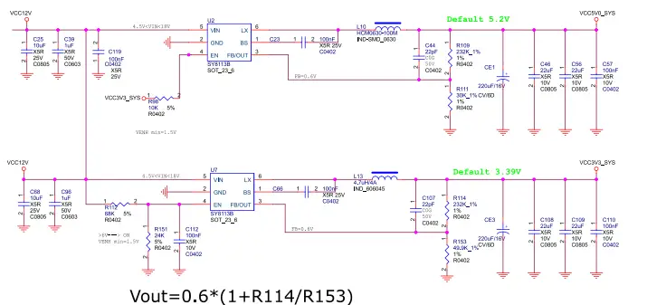
Porohita patuiro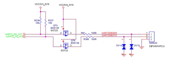
USB OTG Atanga Circuit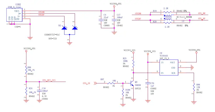
Tapuwae PCB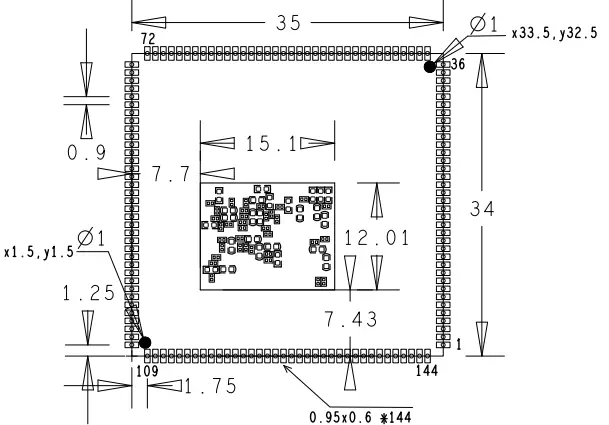
Hua Hunga Hiko
Te Toreretanga me te Pawera
| Tohu | Tawhā | Min | Pato | Max | Waeine |
| VCC3V3_SYS | Pūnaha IO
Voltage |
3.3-5% | 3.3 | 3.3 + 5% | V |
| Isys_in | VCC3V3_SYS tāuru o nāianei | 850 | mA | ||
| Ta | Te Waahi Mahi | -20 | 70 | °C | |
| Tstg | Paemahana Rokiroki | -40 | 85 | °C |
Te Tiakitanga o te Whakamatau
| Te Whakamātautau Whakahaere Teitei | ||
| Ihirangi | Mahi 8h i roto i te pāmahana teitei | 55°C±2°C |
| Hua | TBD |
| Te Whakamatau Ora Whakahaere | ||
| Ihirangi | Te mahi i roto i te ruma | 120h |
| Hua | TBD |
Rarangi Whakaiti
Ka whakamanahia e Boardcon tenei hua kia kore he hapa o nga rawa me nga mahi mo te tau kotahi mai i te ra o te hokonga. I roto i tenei wa whakamana, ka whakatika, ka whakakapi ranei a Boardcon i te waahanga koha ma te mahi e whai ake nei: Me whakauru he kape o te nama taketake ina whakahokia te wae hapa ki a Boardcon. Ko tenei raihana iti e kore e kapi i nga pakaru i puta mai i te uira, i etahi atu hiko hiko, te whakamahi kino, te tukino, nga tikanga rerekee o te mahi, te ngana ranei ki te whakarereke, ki te whakarereke ranei i te mahi o te hua. He iti noa tenei raihana ki te whakatikatika, ki te whakakapi ranei i te waahanga hapa. Karekau he kawenga, he kawenga ranei a Boardcon mo te ngaronga, mo te kino ranei, tae atu ki te kore e iti ki te ngaro o nga hua, nga pakaru ohorere, te pakaru ranei, te ngaronga o nga pakihi, nga hua matakite i puta mai i te whakamahinga, te kore ranei e kaha ki te whakamahi i tenei hua. Ko nga whakatikatika i mahia i muri i te paunga o te wa whakamana ka tau ki te utu whakatikatika me te utu mo te whakahoki mai. Tena koa whakapā atu ki a Boardcon ki te whakarite mo tetahi ratonga whakatika me te whiwhi korero utu whakatika.
FAQ
Q: Me pehea taku whakapai ake i te mahara DDR i runga i te CM1126B-P?
A: Ko te CM1126B-P e tautoko ana ki te 4GB LPDDR4 mahara. Hei whakapai ake, me whakarite te hototahi ki nga whakaritenga me te whai i nga tikanga kua tohua.
Q: He aha te whakaritenga mana hiko mo CM1126B-P?
A: Ko te hiahia mana mo CM1126B-P ko DC 3.3V. Me whakarite ki te whakarato i te hiko hiko i roto i tenei awhe mo te mahi tino pai.
Q: Ka taea e au te whakawhānui ake i te kaha rokiroki o eMMC i runga i te CM1126B-P?
A: Ae, ko te rokiroki eMMC i runga i te CM1126B-P ka taea te whakawhānui ake ki te 256GB. Whakaritea te hototahi ki nga taputapu rokiroki tautoko i mua i te whakahou.
Tuhinga / Rauemi
 |
Papatono Whakamaua CM1126B-P Pūnaha ki te Kōwae [pdf] Pukapuka Kaiwhakamahi V2.20250422, CM1126B-P Pūnaha ki te Kōwae, CM1126B-P, Pūnaha ki te Kōwae, Kōwae |